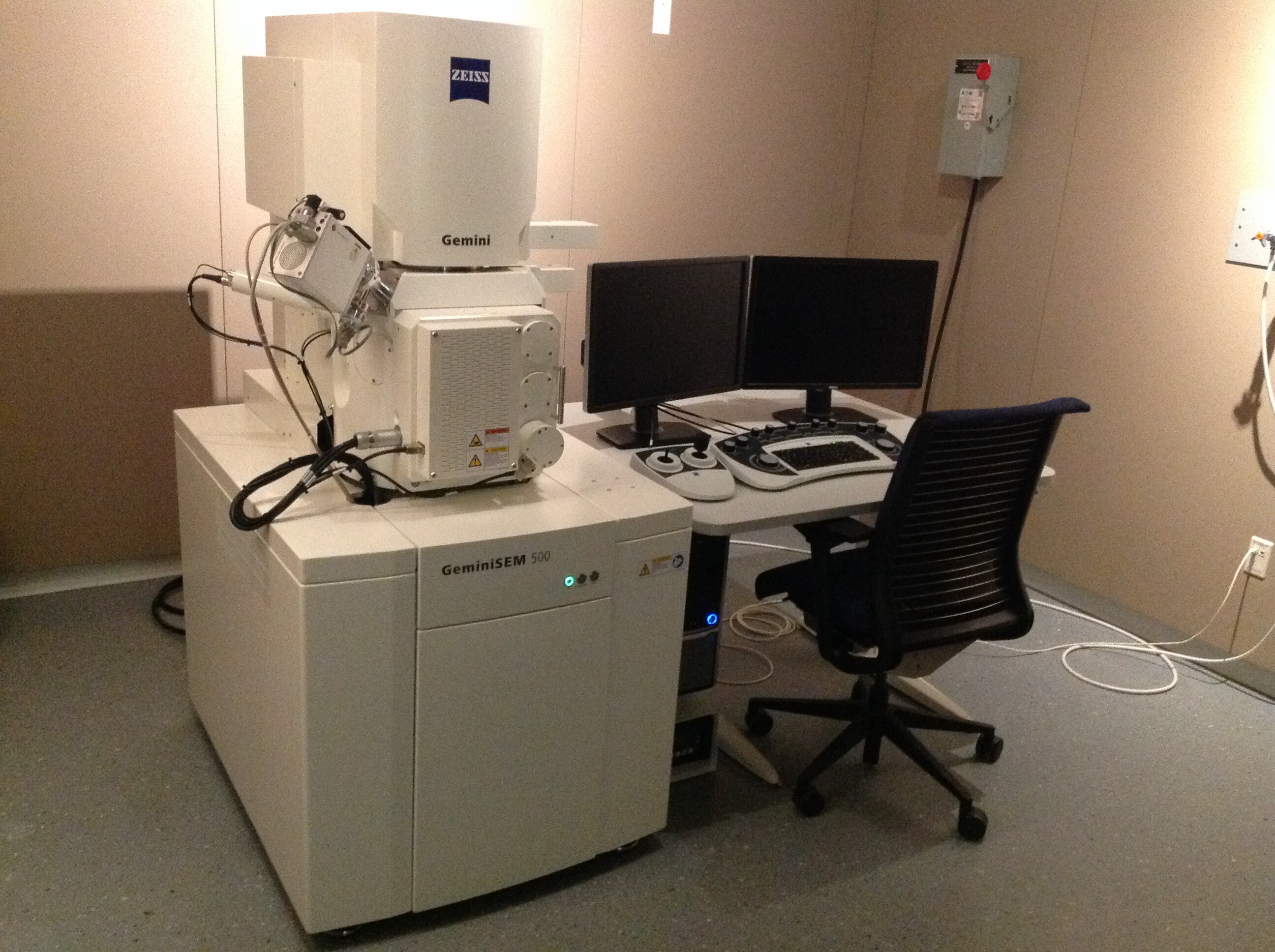
Field Emission Gun Scanning Electron Microscope
Zeiss Gemini SEM 500
The Gemini objective-lens design combines electrostatic and magnetic fields to maximize optical performance while reducing field influences at the sample to a minimum. This enables excellent imaging, even on challenging samples such as magnetic materials.
The Gemini detection concept ensures efficient signal detection by detecting secondary (SE) and backscattered (BSE) electrons in parallel. These so-called Inlens detectors are arranged on the optical axis, reducing the need for realignment, and minimizing time to image.
Gemini beam-booster technology guarantees small probe sizes and high signal-to-noise ratios, right down to very low accelerating voltages.
- Thermal field emission gun type: stability better than 0.2%/h
- Acceleration voltage: 0.02 - 30kv
- Probe current: 3pA to 20nA
- Store resolution: Up to 32k x 24k pixels
- Detectors:
- Inlens Secondary Electron Detector (Inlens)
- Everhart Thornley Secondary Electron Detector (SE2)
- Inlens Energy Selected Backscatter Detector (EsB)
Training is available for students, staff and faculty members.
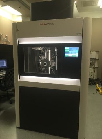
Transmission Electron Microscope
Talos F200C G2 Transmission Electron Microscope
This Life Science TEM on Talos platform is marketed as suitable for nanotechnology research. Large polepeice gap enables cryomicroscopy and tomography at high tilt but with some reduction in resolution. EDS performance will be like a F200i model, which is a general purpose 200 kV Materials Science TEM. Retractable Cryo Shield slows down contamination and allows longer run times and makes EDS installation possible. The constant power lenses make changes from TEM to STEM instantaneous.
This instrument will have a cryo-transfer holder/stage and energy dispersive X-ray spectrometer. Cryo-microscopy is useful for reducing damage rates, minimizing carbon contamination and in soft materials.
Specifications:
Gun type: X-FEG
Gun brightness at 200 kV [A/cm2 /sr] 1.8∙109
Accelerating Voltage: 200kV
TEM information limit: 0.18 nm
TEM point to point resolution: 0.30 nm
Oxford EDAX: AZtec Energy TEM Advanced with X-MaxN TSR 80mm2 with 127eV resolution
Capabilities:
- CryoTEM with long duration dewar
- Scanning Transmission Electron Microscopy (STEM) with EDAX
- Diffraction
- Low Dose Exposure
Training is availble for students, staff and faculty members.
X-RAY Diffractometer
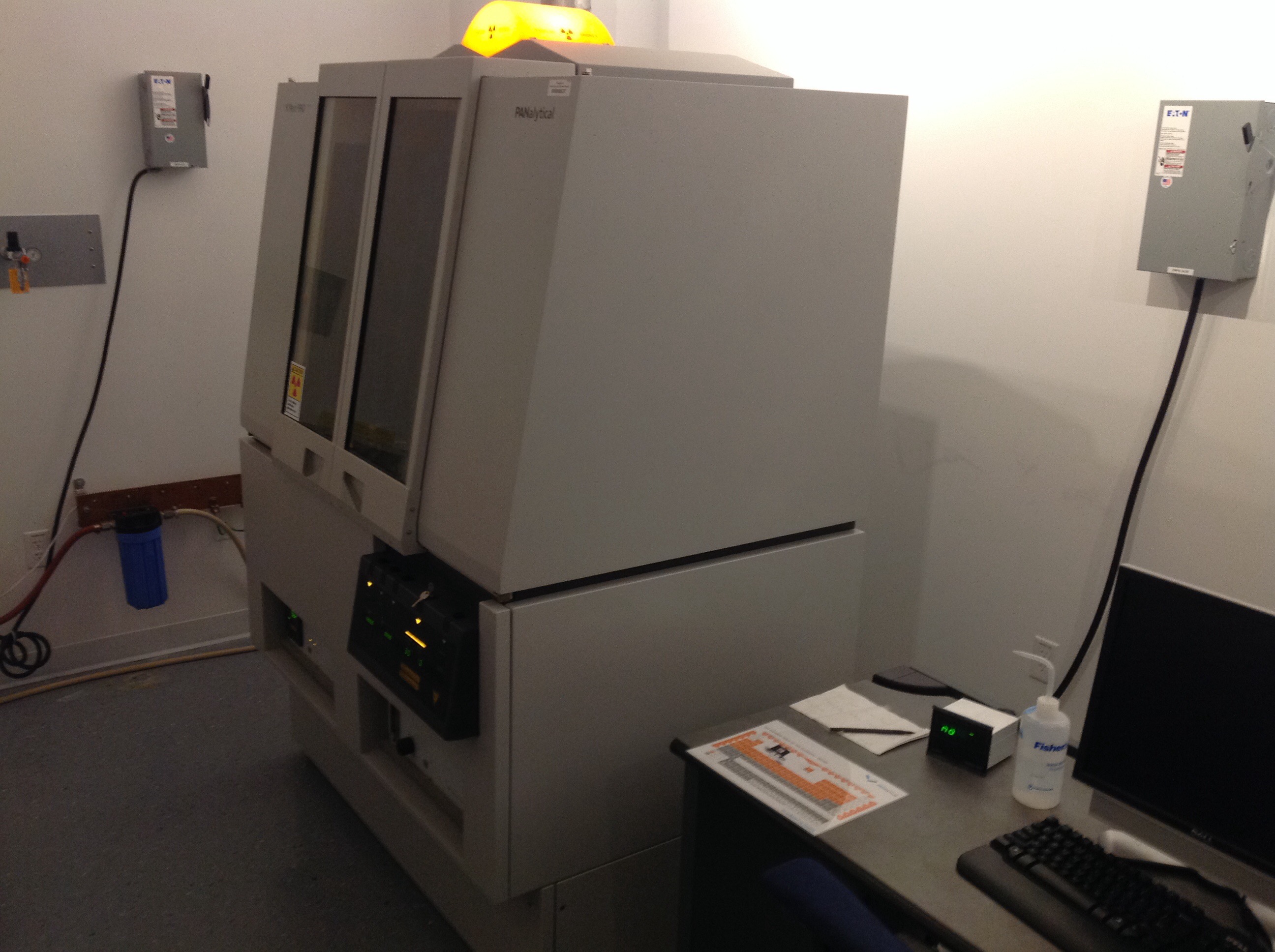
PANalytical X'Pert PRO Theta/Theta Powder X-ray Diffraction System
The PANalytical X'Pert PRO Theta/Theta Powder X-ray Diffraction system with revolutionary X'Celerator detector and 15-position sample changer for high-speed, high-resolution phase analysis features XML-based software for data collection and evaluation, and an Anton Parr TTK 450C temperature chamber.
Other features include:
-
a high-stability, solid-state 3 kW X-ray generator with maximum settings of 60kV and 60mA;
-
Cu and Co tubes;
-
high-performance theta/theta goniometer with accuracy +/- 0.0025 degrees
-
reproducibility of +/- 0.0001 degrees
-
scan speed of 0.001 to 1.27 degrees per second
-
minimum step size of 0.001 degree
-
two-theta measuring range of 0 to 167 degrees; and goniometer radius variable from 130 to 230 mm
-
X'Pert HighScore data analysis software.
Training is available for students, staff and faculty members.
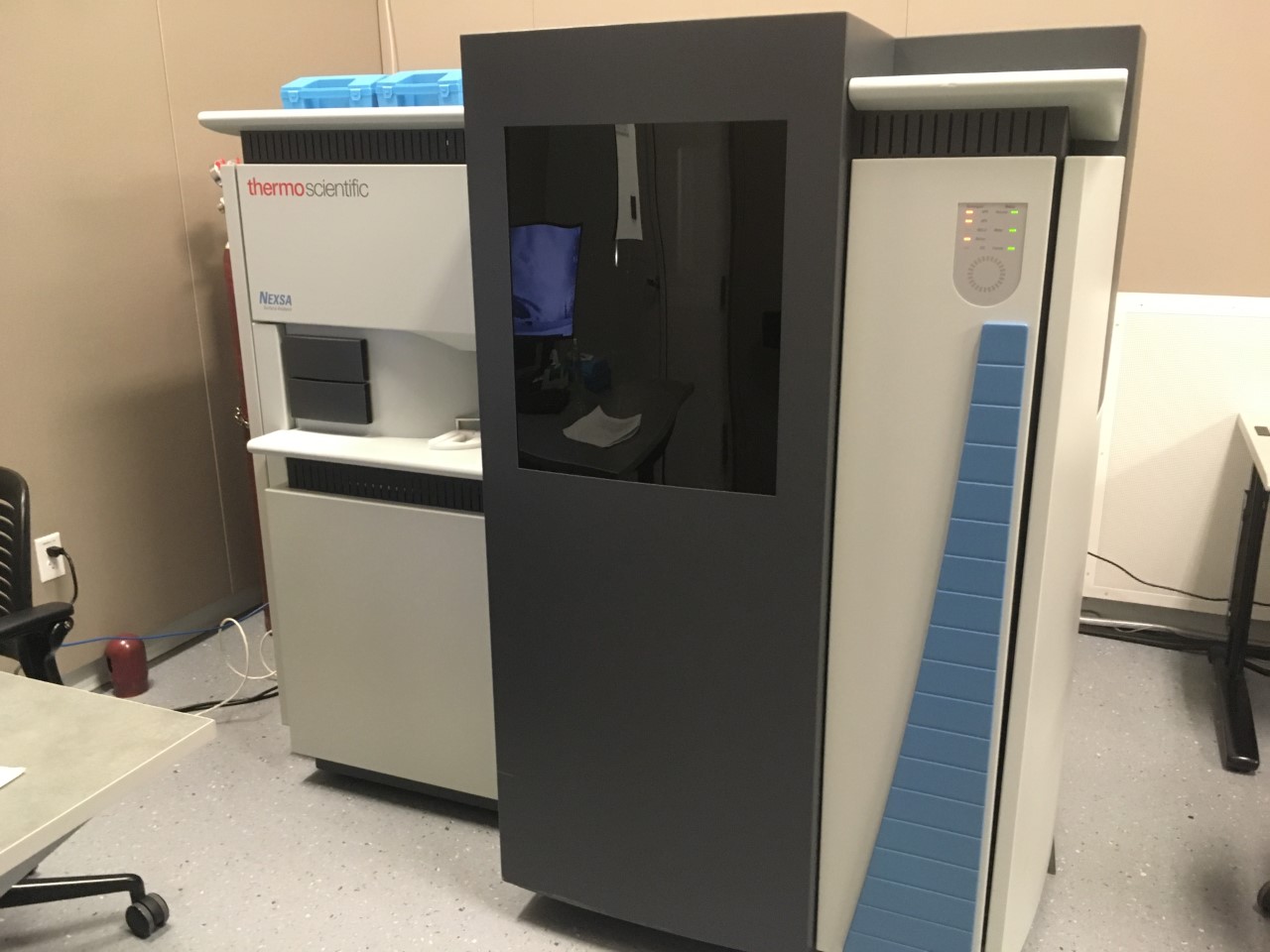
Nexsa X-Ray Photoelectron Spectrometer
Nexus X-Ray Photoelectron Spectrometer (XPS)
A multi-analysis instrument capable of X-Ray Photoelectron Spectroscopy, Ultraviolet Photoelectron Spectroscopy, and Raman Spectroscopy for analysis of surface chemistry of various materials, such as insulators, semiconductors, and metals.
Features include: Insulator analysis, Small spot analysis, and Avantage Software for instrument control, data processing, and reporting
Specifications:
- X-ray Source Type: Monochromated, micro-focused, low power Al Ka X-ray source
- X-ray spot size: 10- 400 µm (adjustable in 5µm steps)
- Analyzer Type: 180°, double-focusing, hemispherical analyser with 128-channel detector
- Sampling Area: 3600 mm2
- Maximum sample thickness: 20 mm
- Depth profiling: EX06 monatomic ion source
- Vacuum System: 2 x 260 260 l.s-1 turbo molecular pumps, with automated titanium sublimation pump, and backing pump
Accessories: UPS, Raman spectrometer
- RAMAN: Spectroscopic technique used to in chemistry to provide a structural fingerprint
- UPS: Ultra-violet photoelectron spectroscopy refers to the measurement of kinetic energy spectra of photoelectrons emitted by molecules which have absorbed ultraviolet photons, in order to determine molecular orbital energies in the valence region
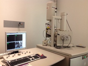
Environmental Scanning Electron Microscope (Currently Offline)
The FEI Quanta 200 ESEM
This environmental scanning electron microscope has a tungsten filament and EDAX Genesis energy-dispersive X-ray spectrometer 30mm2 detector with 132 eV resolution. The microscope has 4 nm spatial resolution and can detect characteristic X-rays down to and including beryllium, although sensitivity is limited for light elements.
It can operate in the low-vacuum range (10-3 to 0.8 Torr) and in environmental mode (0.1 to 40 Torr). In the environmental mode, it is possible to examine samples from at 100 percent relative humidity, making this a highly versatile instrument.
The EDAX Genesis software allows the user to collect spectra and elemental maps in both manual and automated modes. With this instrument, it is possible to view and perform X-ray analysis on non-conducting samples or "wet samples" without having to coat or dry.
Training is available for students, staff and faculty members.